
 USA
USA English
 日本語
日本語 中文简体
中文简体
Content
- 1 What Is ESD Masking Tape?
- 2 Why Standard Masking Tape Is Not Acceptable in EPA Environments
- 3 Construction and Material Options for ESD Masking Tape
- 4 Key Process Applications in Electronics Manufacturing
- 5 ESD Standards and Compliance Requirements
- 6 Specification Checklist When Sourcing ESD Masking Tape
What Is ESD Masking Tape?
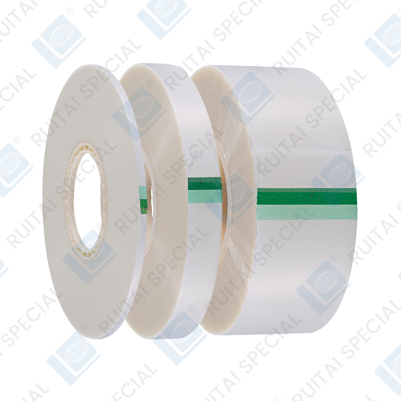
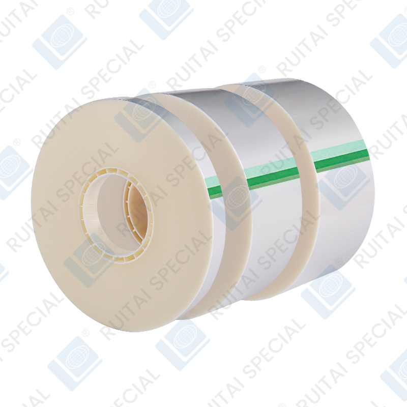
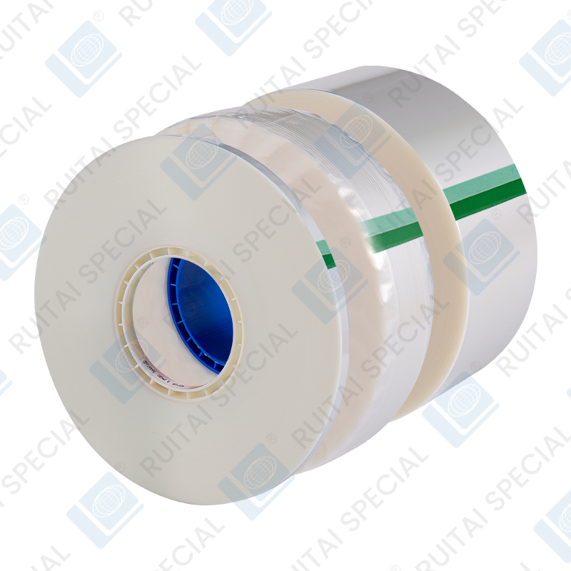
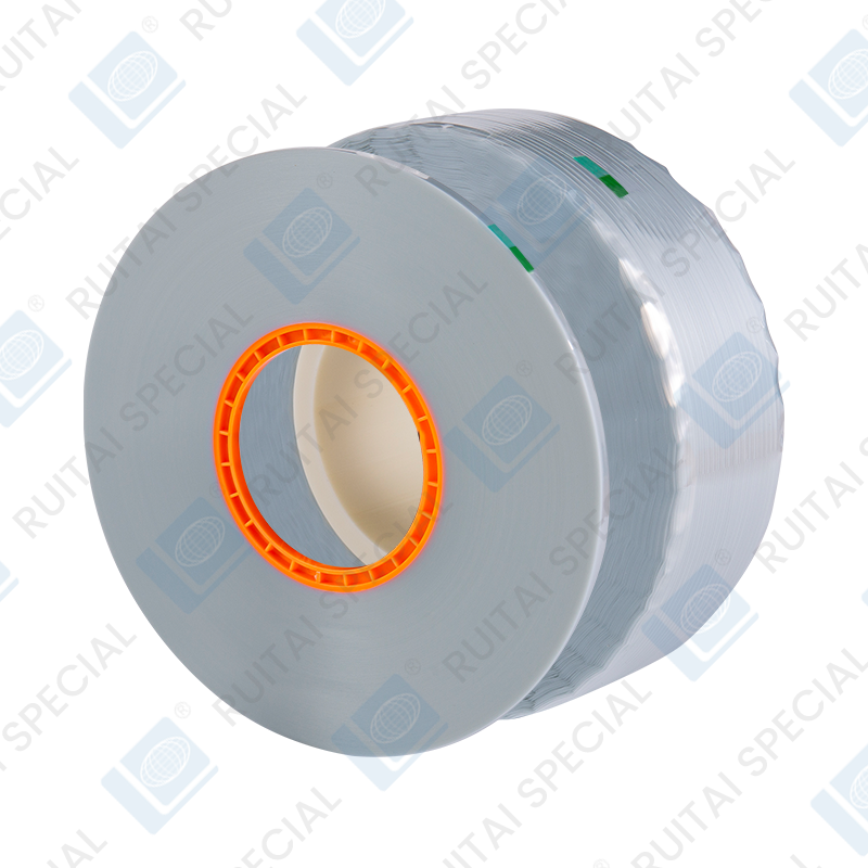
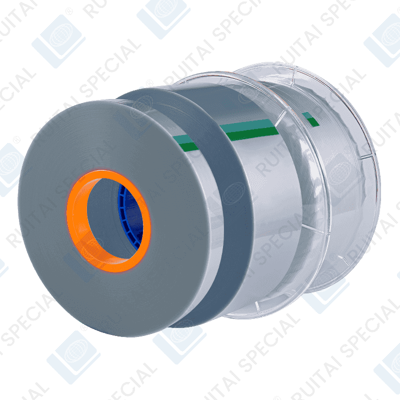
ESD masking tape is a pressure-sensitive adhesive tape engineered to control electrostatic discharge (ESD) during masking operations in electronics manufacturing and PCB assembly environments. Unlike standard masking tapes, which can accumulate and release static charges when applied or removed — potentially damaging sensitive components — ESD masking tape is formulated with electrically conductive or dissipative materials that prevent the buildup of triboelectric charge throughout its use.
The tape performs a dual function: it acts as a conventional masking medium — protecting specific areas of a PCB, connector, or substrate from solder, conformal coating, paint, or plating — while simultaneously maintaining a controlled surface resistivity that keeps the work area ESD-safe. This dual role makes it indispensable in wave soldering, selective conformal coating, reflow processes, and any masking step performed inside an ESD-protected area (EPA).
Surface resistivity of ESD masking tape typically falls within the dissipative range of 10⁶ to 10¹¹ ohms per square, as defined by ANSI/ESD S20.20 and IEC 61340-5-1 standards. Tapes with surface resistivity below 10⁶ Ω/sq are classified as conductive and may be specified for high-sensitivity grounding applications; those above 10¹¹ Ω/sq cross into the insulative range and cannot be used in ESD-protected environments.
Why Standard Masking Tape Is Not Acceptable in EPA Environments
Conventional masking tapes — including general-purpose crepe paper tape, standard polyimide tape, and PTFE tape — are electrically insulative. Their surface resistivity typically exceeds 10¹² to 10¹⁴ Ω/sq, placing them firmly in the insulator category. When these tapes are peeled, repositioned, or even rubbed by gloved hands, triboelectric charging can generate electrostatic potentials of several hundred to several thousand volts on the tape surface or on the workpiece beneath it.
The consequences are well-documented: latent ESD damage to CMOS devices, gate oxide degradation in MOSFETs, dielectric breakdown in multilayer ceramic capacitors (MLCCs), and functional failures in RF components that may not manifest until field deployment. Because latent damage does not cause immediate functional failure, it often escapes end-of-line testing — resulting in field returns, warranty costs, and brand reputation damage that far exceeds the cost of the masking operation itself.
IEC 61340-5-1 explicitly classifies insulators as ESD hazards in protected areas and requires that any item introduced into an EPA — including tapes, labels, and masking materials — either demonstrate dissipative surface properties or be kept at a minimum distance of 30 cm from ESDS (ESD-sensitive) devices. In practice, masking operations on assembled PCBs cannot maintain a 30 cm separation, making ESD masking tape the only compliant solution.
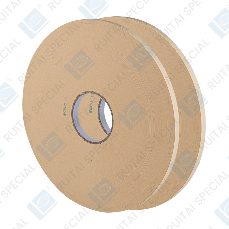
Construction and Material Options for ESD Masking Tape
ESD masking tapes are available in several backing material and construction configurations, each optimized for a specific process temperature, chemical exposure, or surface geometry.
ESD Polyimide (Kapton) Masking Tape
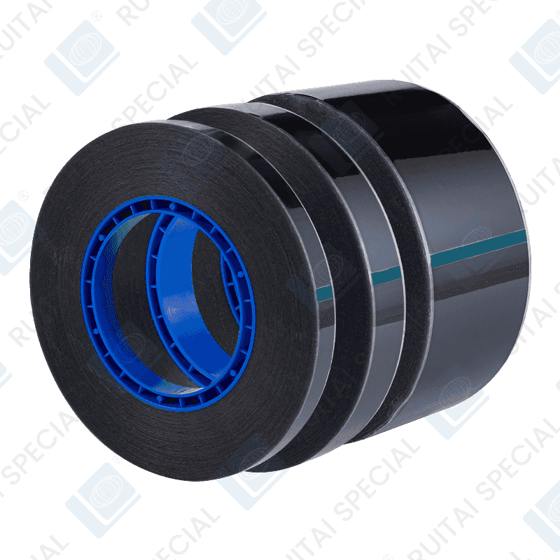
Polyimide film backing treated with carbon-loaded or inherently dissipative coatings is the most widely used ESD masking tape construction in SMT and wave soldering. Standard polyimide tape already offers excellent thermal stability (continuous service to 260°C, with short-term peaks to 300°C+) and chemical resistance to fluxes and solvents. The ESD version adds a dissipative surface layer — typically a carbon-dispersed acrylic or inherently conductive polymer coating — that brings surface resistivity into the 10⁶–10¹⁰ Ω/sq range without compromising thermal or chemical performance.
ESD Crepe Paper Masking Tape
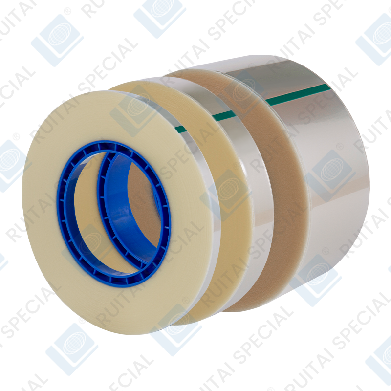
For lower-temperature masking operations (typically up to 120–150°C), ESD crepe paper tape provides a cost-effective dissipative masking medium. The paper backing is impregnated or surface-coated with carbon or conductive polymer to achieve dissipative resistivity. It conforms well to curved surfaces and is easily torn by hand, making it practical for manual masking in high-mix, low-volume production environments. It is not suitable for reflow oven or wave solder applications where temperatures exceed its thermal limit.
ESD PET Film Masking Tape
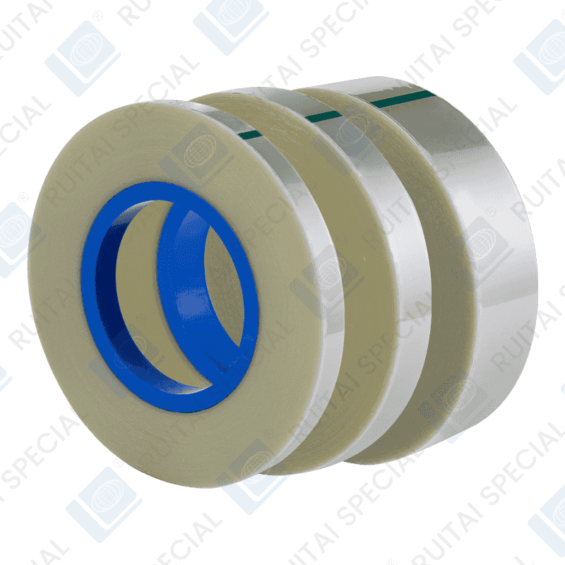
Polyester (PET) film backing with dissipative coating offers a balance between the dimensional stability and smooth surface of film tapes and a more economical price point than polyimide. PET-based ESD masking tape handles temperatures to approximately 150°C and is well-suited for selective conformal coating masking on connectors and test points where precise edge definition is required. The non-conformable nature of PET film makes it less suitable for complex three-dimensional masking geometries.
ESD Foam and Specialty Constructions
For component protection during handling — rather than process masking — ESD polyethylene foam tape and ESD conductive cloth tape are used. Conductive cloth tape (typically carbon-fiber or metallic-fiber woven backing with conductive adhesive) achieves surface resistivity below 10⁴ Ω/sq and is used for grounding straps, EMI shielding gasket attachment, and cable bundle grounding rather than masking in the traditional sense.
| Backing Type | Max. Temp. | Surface Resistivity | Typical Use |
|---|---|---|---|
| ESD Polyimide (PI) | 260–300°C | 10⁶–10¹⁰ Ω/sq | SMT reflow, wave solder, flex circuit masking |
| ESD Crepe Paper | 120–150°C | 10⁶–10¹¹ Ω/sq | Manual masking, low-temp coating ops |
| ESD PET Film | 130–150°C | 10⁶–10¹⁰ Ω/sq | Conformal coating, connector masking |
| ESD Conductive Cloth | 80–120°C | <10⁴ Ω/sq | Grounding, EMI shielding, cable bonding |
Key Process Applications in Electronics Manufacturing
ESD masking tape is used across multiple process steps in PCB assembly and electronic device manufacturing. Each application places distinct requirements on the tape's thermal stability, adhesion level, residue profile, and dimensional stability.
Wave Soldering and Selective Soldering Masking
During wave soldering, ESD polyimide masking tape is applied over connectors, switches, battery contacts, and other through-hole components that must remain solder-free. The tape must withstand contact with molten solder at 250–270°C without adhesive bleed, delamination, or backing distortion, and must remove cleanly after the solder pass without leaving adhesive residue on gold or silver-plated contacts. Residue-free clean removal is a defining quality criterion for high-reliability wave solder masking tape.
Conformal Coating Masking
Selective conformal coating — applying acrylic, polyurethane, silicone, or epoxy coating to protect PCBs from moisture, fungus, and contamination — requires precise masking of connectors, test points, mounting holes, and adjustment components that must remain uncoated. ESD masking tape used in this application must seal the masked edge cleanly to prevent coating bleed-under while remaining removable after UV or thermal cure cycles without pulling solder joints or pad finishes from the board surface.
Reflow Oven and Thermal Process Masking
In double-sided SMT reflow, the second reflow pass subjects previously soldered bottom-side components to temperatures above 200°C. ESD masking tape used to protect delicate components or label areas on the bottom side must maintain adhesion and backing integrity through two complete reflow cycles while preventing component shift or contamination from adhesive migration.
Electrostatic-Sensitive Component Handling and Packaging
Beyond in-process masking, ESD tape is used to secure ESD-sensitive devices in trays and carriers during transport between workstations, to seal ESD shielding bags after component withdrawal, and to label ESD-sensitive assemblies with warning indicators. In these applications, the primary requirement is dissipative surface resistivity and clean adhesion to shielding bag materials rather than thermal performance.
ESD Standards and Compliance Requirements
Selecting ESD masking tape for a certified EPA requires verifying compliance with applicable industry standards. The two dominant ESD control standards globally are ANSI/ESD S20.20 (widely adopted in North America and internationally) and IEC 61340-5-1 (European and global standard). Both define the surface resistivity requirements for materials used in EPAs and require that dissipative materials fall within the 10⁶–10¹¹ Ω/sq range.
Additional test methods relevant to ESD masking tape qualification include:
- ANSI/ESD STM11.11 — surface resistance measurement of planar materials using concentric ring electrode method
- ANSI/ESD STM11.12 — volume resistance of materials
- IEC 61340-4-1 — measurement of surface resistance and resistivity using a standard electrode configuration
- ASTM D257 — DC resistance and conductance of insulating materials (commonly referenced for volume and surface resistivity benchmarking)
Reputable ESD masking tape suppliers provide a Technical Data Sheet (TDS) and ESD compliance test report specifying measured surface resistivity values, test method used, and electrode configuration. Buyers should request third-party test data — not only manufacturer-stated specifications — when qualifying tape for use in high-reliability defense, medical, or aerospace electronics manufacturing environments.
Specification Checklist When Sourcing ESD Masking Tape
Procurement teams and process engineers qualifying a new ESD masking tape supplier or product should evaluate the following parameters against their specific process requirements:
- Surface resistivity (Ω/sq) — verify measured value falls within 10⁶–10¹¹ Ω/sq range; request test report citing specific ANSI/ESD or IEC method used
- Maximum service temperature — must exceed peak process temperature with a safety margin of at least 20°C; for wave solder masking, confirm rated performance at 260°C minimum
- Adhesion level — peel strength (N/25mm) to relevant substrate (FR4, gold plating, aluminium housing); too high risks substrate damage on removal, too low risks solder or coating bleed-under
- Residue performance — confirm clean removal after maximum process exposure time and temperature; request residue test data on gold, ENIG, and OSP surface finishes if applicable
- Dimensional stability — thermal elongation or shrinkage of the backing at process temperature affects masking edge definition; critical for fine-pitch connector masking and SMD land protection
- Halogen content — RoHS compliance and halogen-free declaration required for most consumer electronics OEM supply chains; confirm IEC 61249-2-21 or equivalent certification
- Shelf life and storage conditions — pressure-sensitive adhesives degrade with time, temperature, and humidity; confirm shelf life (typically 12–24 months) and storage requirements (typically 21°C ±3°C, 50% RH ±5%)