 USA
USA English
 日本語
日本語 中文简体
中文简体
Content
- 1 What Antistatic Protection Tape Does — and Why It Matters in Electronics Manufacturing
- 2 How Antistatic Tape Works: Surface Resistivity and Charge Dissipation
- 3 Common Substrates and Backing Materials
- 4 Key Selection Criteria for Antistatic Protection Tape
- 5 Where Antistatic Protection Tape Is Used in Practice
What Antistatic Protection Tape Does — and Why It Matters in Electronics Manufacturing
Antistatic protection tape is a pressure-sensitive adhesive tape engineered to prevent the buildup and discharge of electrostatic charge on or near sensitive components. A single electrostatic discharge (ESD) event of as little as 100 volts can permanently damage or degrade a semiconductor device — yet the human body can accumulate 35,000 volts simply by walking across a carpeted floor. Standard tapes, even those made from inert materials, generate triboelectric charge during unwind and application, introducing an ESD risk at the very moment components should be protected. Antistatic tape eliminates that risk by dissipating charge rather than accumulating it.
The tape is used across PCB assembly, semiconductor packaging, SMT (surface mount technology) reflow processes, tape-and-reel carrier systems, wafer handling, and medical device manufacturing — anywhere that an uncontrolled discharge could compromise yield, reliability, or safety compliance.
How Antistatic Tape Works: Surface Resistivity and Charge Dissipation
The functional property of antistatic protection tape is measured by surface resistivity, expressed in ohms per square (Ω/sq). The ESD Association (ESDA) and IEC 61340 standards define three material categories relevant to tape selection:
- Conductive: Surface resistivity below 105 Ω/sq. Dissipates charge nearly instantaneously — suitable for grounding straps and shielding layers, but too aggressive for direct contact with sensitive ICs.
- Dissipative (ESD-safe): Surface resistivity between 105 and 1011 Ω/sq. The preferred range for most antistatic protection tapes — charge bleeds away in a controlled, non-damaging manner. This is the standard specification for tapes used in semiconductor packaging and SMT processes.
- Antistatic (charge-generating inhibitor): Surface resistivity above 1011 Ω/sq. Does not conduct electricity but resists triboelectric charge generation — typically used for packaging films and surface liners rather than load-bearing protective tape.
Most antistatic protection tapes achieve their dissipative behavior through one of two methods: carbon-loaded or metallic filler compounding in the backing material, or topical antistatic coating applied to the film surface. Carbon-filled formulations offer more durable and humidity-independent performance; topical coatings are lower cost but can degrade with abrasion or over time.
Common Substrates and Backing Materials
Antistatic protection tapes are manufactured on a range of backing materials, each suited to different process conditions:
| Backing Material | Key Properties | Typical Applications |
|---|---|---|
| Polyimide (PI / Kapton) | High-temp resistance (up to 260°C), dimensionally stable | SMT reflow masking, PCB wave soldering |
| PET (Polyester) | Good tensile strength, low outgassing, cost-effective | Component taping, reel splicing, wafer handling |
| Polyethylene (PE) Foam | Cushioning, conformable, absorbs mechanical shock | PCB edge protection, component tray lining |
| Fabric / Woven | High tear strength, flexible, breathable | Harness bundling, cable wrapping in ESD-sensitive environments |
| Acetate / Crepe | Hand-tearable, moderate temperature resistance | Masking during conformal coating, general ESD taping |
Key Selection Criteria for Antistatic Protection Tape
Choosing the right antistatic tape involves matching the tape's properties to the specific process environment rather than applying a single universal specification. The most important parameters to evaluate:
Surface Resistivity Range
Confirm the tape meets the resistivity class required by your process specification — typically IEC 61340-5-1 or ANSI/ESD S20.20. For direct contact with ESDS (ESD-sensitive) components, dissipative range (105–1011 Ω/sq) is almost always the correct choice, as conductive materials can create unwanted current paths through sensitive circuits.
Temperature Resistance
For any application involving reflow ovens, wave soldering, or autoclave processes, the tape must maintain both its adhesive bond and its ESD properties at process temperature. Polyimide-backed tapes with silicone adhesive are standard for lead-free reflow profiles that reach 260°C peak; PET-backed tapes are limited to approximately 130–150°C.
Adhesive Type and Residue Performance
In semiconductor and PCB applications, adhesive residue after tape removal is a critical defect risk. Silicone adhesives offer the cleanest removal on most substrates but can cause contamination issues in optical or coating processes. Acrylic adhesives have lower residue risk in high-humidity environments and are generally preferred for cover tape and reel-carrier applications. Always verify residue performance against your specific substrate before production use.
Compliance and Certification
For regulated industries or export markets, confirm that the tape is compliant with RoHS (EU Directive 2011/65/EU) and REACH SVHC requirements. Medical device manufacturers additionally require tapes with documented biocompatibility data and traceability. ESD performance certification to IEC 61340 or JEDEC standards is typically required for semiconductor packaging customers.
Where Antistatic Protection Tape Is Used in Practice
The applications for antistatic protection tape extend across every stage of the electronics supply chain:
- SMT masking: Taping over connectors, edge contacts, and gold fingers during wave soldering or conformal coating to protect surfaces while maintaining ESD-safe handling throughout the assembly line.
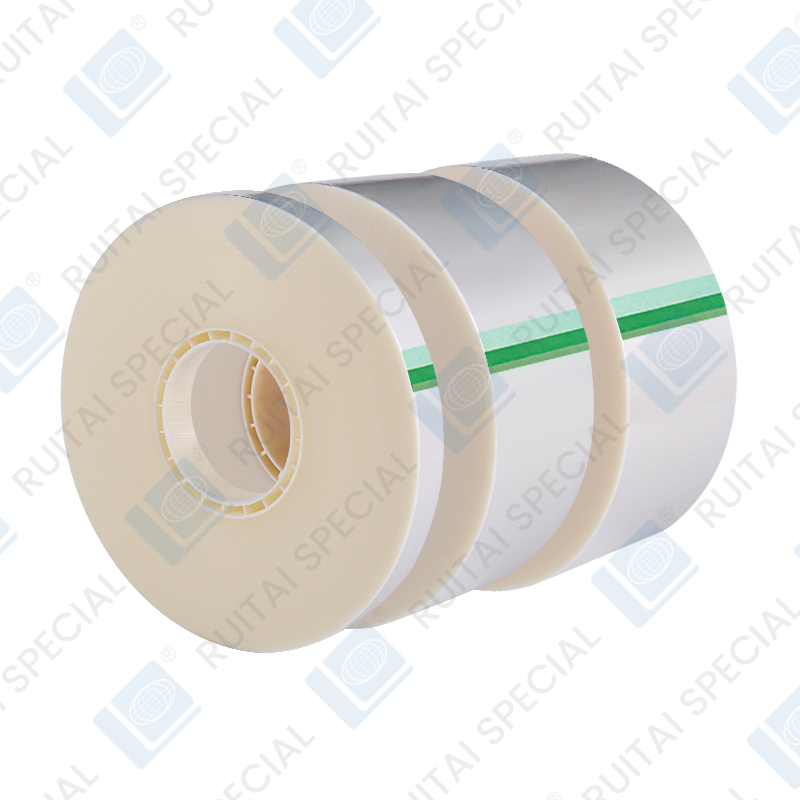
- Tape-and-reel carrier systems: Cover tape on embossed carrier reels used to feed components into pick-and-place machines must be antistatic to prevent charge buildup during high-speed unwind — a frequent but overlooked ESD source in automated assembly.
- Wafer and die handling: Backgrinding tape and dicing tape used in wafer processing are antistatic by design; any charge accumulated during the dicing process transfers directly to the die surface and can damage gate oxides.
- PCB storage and transport: Antistatic tape seals ESD shielding bags and secures PCBs within anti-static foam trays during shipping, maintaining the integrity of the overall ESD protective packaging system.
- Cleanroom environments: Low-outgassing antistatic tapes are used in ISO Class 5–7 cleanrooms for cable management, equipment labeling, and temporary fixturing where conventional tapes would introduce contamination.
 HAA cover tape with hazy surface")
 HAA cover tape with transparent surface")
,wide size HAA cover tape with transparent surface")
 HAA cover tape with transparent surface")
 HAA cover tape with transparent surface")


